Technology
BSP has been developing core technologies and solutions for more than 10 years and leverages these capabilities to propose solutions to satisfy customers' needs and wants.
ISB®
Selective Bonding thru Induction
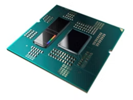
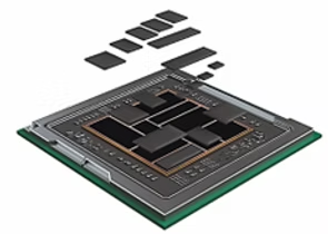
ISB®, a technology developed and patented by BSP, is a room temperature non-contact magnetic induction bonding method that enables various multi-chips and stacked die simultaneously. This is a technology and equipment that can be used in numerous industries in the future as it can cope with devices vulnerable to heat and pressure or semiconductor chip bonding and can improve bending during semiconductor bonding of large die sizes. This is the best solution that can be applied to heterojunction technology, which is the highlight of recent bonding technology
Through our ISB®(Selective Bonding Thru Induction) technologies, we can provide services tailored to our customers' needs and wants in the areas of semiconductors.
Characteristics of ISB®
● Low pressure / indirect heating soldering
● Response to heat- and pressure-sensitive devices or semiconductor chip bonding
● Improvement of bending in large die size semiconductor bonding
● Multiple chips can be joined simultaneously
● Selective heating minimizes thermal effects on other circuits in the substrate
Advantage of ISB®
● Meets tight production tolerances with precise localized heat to small areas creating pinpoint accuracy
● Increases production rates with faster heating cycles
● Reduces defect rates with repeatable, reliable heat
● Eliminates variability from operator-to-operator, shift-to-shift
● Maintains metallurgical characteristics of the individual metals
● Can be joined at non-contact or low pressure
● Local heating furnace die thermal damage written only on solder pad side
● Improved chip performance due to low thermal damage accumulation
MDM®
Direct Mounting Technology
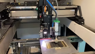
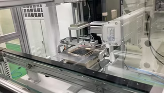
MDM® is an optional and selective soldering method that minimizes thermal damage to the subject by utilizing the room temperature non-contact soldering technique.
SIMULATION Heating Simulation
MP DESIGN Production Design
DISPENSING Putting exactly accurate amount of solder by using non-contacted jetting method
MOUNTING Pick up components and locate in the soldering position
SOLDERING Room temperature, non-contact soldering
LCT
Laser Circuit Technology
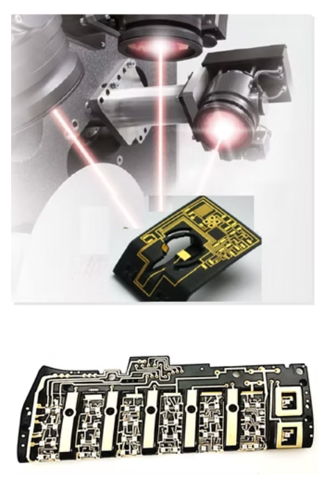
LCT(Laser Circuit Technology) offers a viable alternative to the harness and wiring of conventional PCB and FPCB components, improving connectivity and offering a replacement for traditional components.
The assembly process for traditional PCB and FPCB components is streamlined, leading to increased efficiency and cost savings.
Expect enhanced efficiency and cost-effectiveness through the simplified assembly process. LCT provides optimized solutions with various materials suitable for diverse industries and applications.
Explore the capabilities of three-dimensional circuits, offering a range of functionalities tailored for various industries and applications.
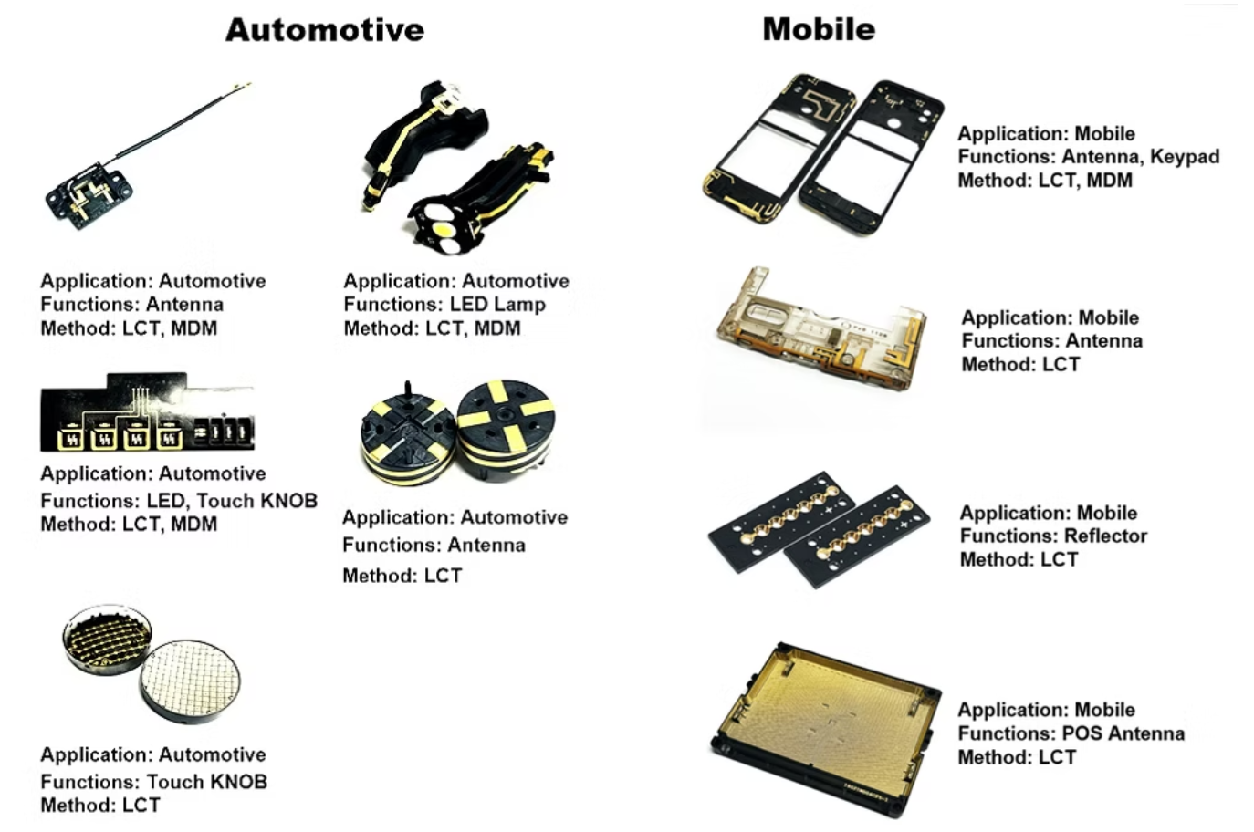
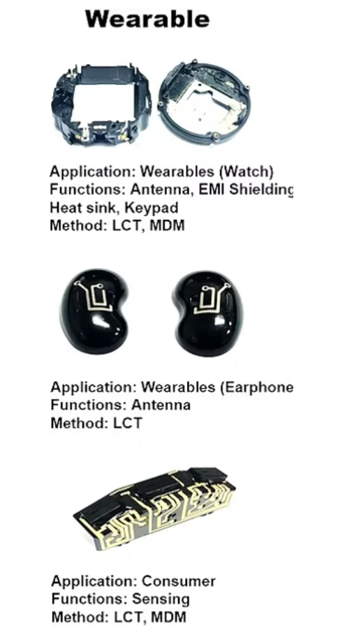
Application
BSP develops and provides various solutions with its patented technologies that customers want with its own developed products. These solutions will provide reliable, easily applicable and cost-competitive solutions to customers who produce a wide range of products.
Solutions with LCT and MDM® Technology
Developed and patented by BSP, LCT and MDM technologies are very specialized solutions for developing various products and parts of customers. This allows customers to develop quality, cost, and reliability products to satisfy their customers.